Semicon 2.0: India’s Semiconductor Mission, Chips, Fabs, Packaging and Strategic Importance
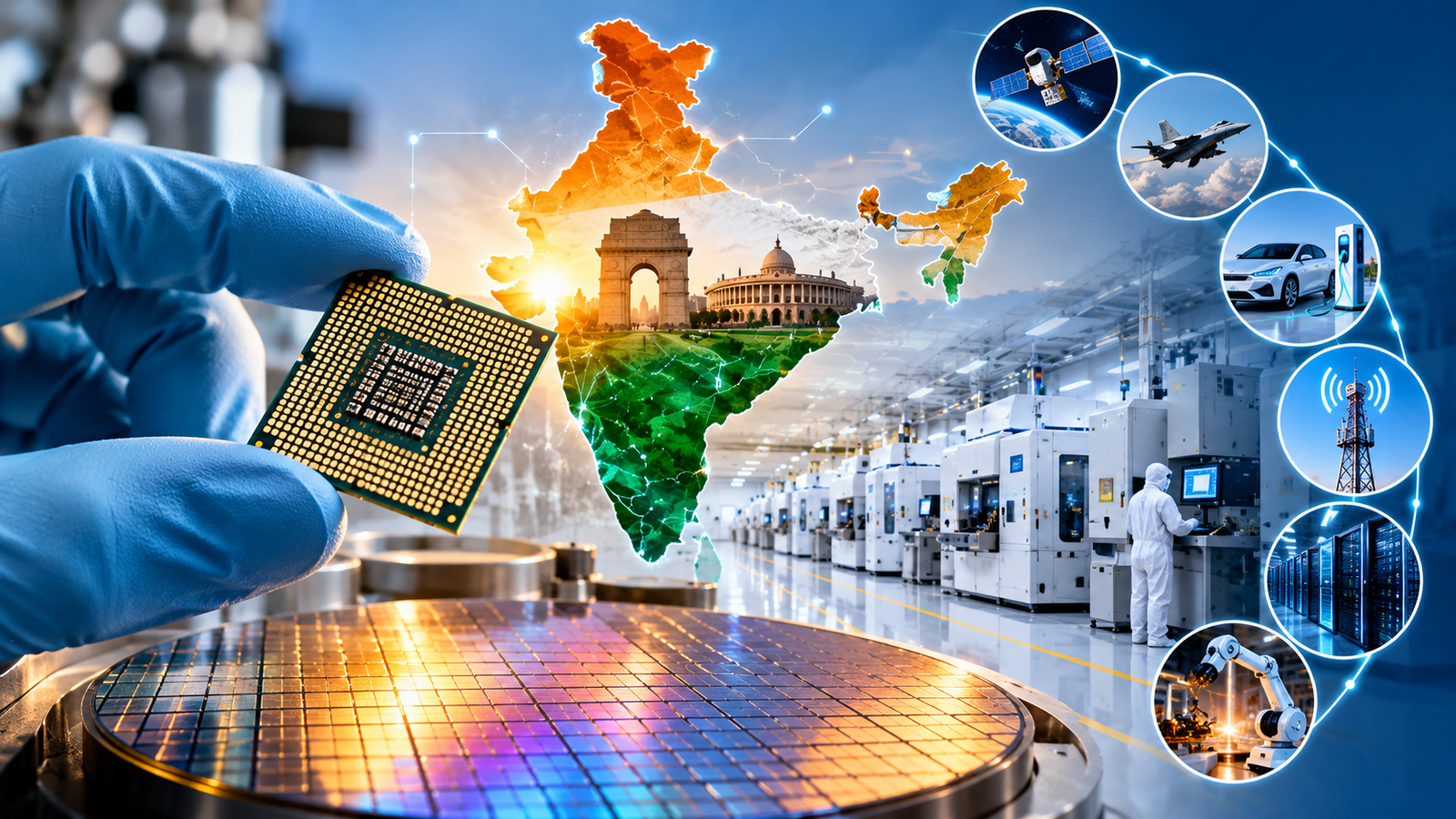
Semiconductors are the tiny building blocks behind almost every modern technology—from smartphones and computers to electric vehicles, satellites, defence systems, artificial intelligence and data centres.
Recognising their strategic importance, the Government of India approved Semicon 2.0 on 15 July 2026 with a total outlay of ₹1,27,500 crore. The programme aims to move India beyond individual semiconductor projects and build a complete semiconductor ecosystem covering design, manufacturing, equipment, materials, advanced packaging, research and talent.
The development is important for UPSC because semiconductors connect Science & Technology, Economy, National Security, Geopolitics, Critical Supply Chains, Artificial Intelligence and Atmanirbhar Bharat.
Why Is Semicon 2.0 in News?
The Union Cabinet approved Semicon 2.0 in July 2026 with an outlay of ₹1,27,500 crore.
The programme builds upon Semicon 1.0, which laid the foundation for semiconductor manufacturing in India.
The new phase aims to develop the entire semiconductor value chain through six broad pillars:
- Chip design
- Semiconductor machines and materials
- More fabrication facilities
- Advanced ATMP/OSAT facilities
- Research and development
- Talent development
The latest government assessment shows that India’s semiconductor ecosystem has already moved from the policy stage towards actual production: 12 semiconductor manufacturing units have been approved, with investment commitments exceeding ₹1.64 lakh crore, and five units had commenced commercial production by September 2026.
First Understand: What Is a Semiconductor?
Before understanding Semicon 2.0, it is important to understand the basic concept.
A semiconductor is a material whose electrical conductivity can be controlled.
It lies between:
Conductors
Materials such as copper that allow electricity to flow easily.
and
Insulators
Materials that strongly resist the flow of electricity.
The most widely used semiconductor material is silicon.
Semiconductors can be engineered to:
- switch electrical signals;
- amplify signals;
- sense physical conditions;
- control electrical power;
- process information.
Modern semiconductor chips contain enormous numbers of microscopic components called transistors.
What Is a Transistor?
A transistor is a tiny electronic switch that controls the flow of electrical current.
A simple way to understand it is:
ON → 1
OFF → 0
These combinations of 1s and 0s form the basis of digital computing.
Modern processors contain millions or billions of transistors.
Therefore:
Semiconductor → Transistor → Integrated Circuit → Computer Processing
This is why semiconductors are often called the building blocks of modern electronics.
What Is a Semiconductor Chip?
A semiconductor chip is a small piece of semiconductor material containing a large number of electronic components, particularly transistors.
A chip can perform functions such as:
- processing information;
- storing information;
- controlling machines;
- communicating signals;
- managing electrical power;
- sensing physical conditions.
Chips are therefore used in:
- smartphones;
- laptops;
- automobiles;
- medical equipment;
- satellites;
- defence systems;
- telecom networks;
- industrial machinery;
- AI systems;
- data centres.
From Sand to Semiconductor Chip
This is an excellent conceptual topic for UPSC.
Silicon is obtained from silica, which is abundant in nature.
The broad semiconductor manufacturing process can be simplified as:
Silica
↓
Highly purified silicon
↓
Silicon ingot
↓
Wafer
↓
Photolithography + Deposition + Etching + Ion Implantation
↓
Transistors and circuits
↓
Testing
↓
Packaging
↓
Finished chip
Actual fabrication involves hundreds of highly controlled processes.
What Is a Wafer?
A wafer is a thin, flat disc of semiconductor material, usually silicon, on which electronic circuits are fabricated.
Think of it as a large platform containing many individual chips.
After the circuits are manufactured, the wafer is divided into individual units called dies.
These dies are then packaged and tested.
What Is a Fab?
Fab is short for fabrication facility.
A semiconductor fab is a highly specialised manufacturing facility where semiconductor wafers are processed to create integrated circuits.
A fab requires:
- ultra-clean environments;
- advanced machinery;
- extremely pure materials;
- specialised chemicals and gases;
- sophisticated water systems;
- highly skilled engineers;
- precise temperature and contamination control.
Semiconductor fabrication is therefore among the world’s most complex manufacturing activities.
What Is Semiconductor Fabrication?
Fabrication is the process through which electronic circuits are physically created on a semiconductor wafer.
Major processes include:
Photolithography
Patterns are transferred onto the wafer using light.
Deposition
Very thin layers of material are deposited on the wafer.
Etching
Unwanted material is removed to create the required structures.
Ion Implantation
Specific ions are introduced into the semiconductor to modify its electrical properties.
These processes are repeated across multiple layers to build complex integrated circuits.
What Is a Semiconductor Node?
You will frequently see terms such as:
28 nm, 14 nm, 7 nm, 5 nm, 3 nm
These refer to process nodes.
Historically, node numbers were more directly associated with particular physical dimensions of transistor structures. Today, however, node names primarily act as labels for different generations of semiconductor manufacturing technology.
Generally, more advanced nodes can allow:
- higher transistor density;
- improved performance;
- lower energy consumption.
However, a smaller node does not automatically mean a better chip for every application.
Mature nodes remain extremely important for:
- automobiles;
- industrial electronics;
- telecommunications;
- power systems;
- consumer electronics.
This is an important UPSC conceptual point.
What Is Semiconductor Packaging?
Fabrication creates the semiconductor device, but the chip still needs to be protected and connected to other electronic components.
This is where packaging becomes important.
Packaging:
- protects the chip;
- provides electrical connections;
- helps manage heat;
- enables integration with other components.
After fabrication, semiconductor devices undergo processes such as:
Assembly → Testing → Marking → Packaging
This is commonly abbreviated as ATMP.
Another term you will encounter is:
OSAT
Outsourced Semiconductor Assembly and Test
OSAT companies provide assembly and testing services for semiconductor manufacturers.
ATMP vs OSAT
ATMP
Assembly, Testing, Marking and Packaging
It refers to the set of processes involved in finishing semiconductor devices after fabrication.
OSAT
Outsourced Semiconductor Assembly and Test
It refers to specialised companies that provide these services on an outsourced basis.
Semicon 2.0 seeks to strengthen India’s ATMP/OSAT ecosystem and bring more advanced packaging technologies into the country.
Why Are Semiconductors Strategically Important?
Semiconductors are no longer just an industrial commodity.
They have become a strategic resource.
They are essential for:
Artificial Intelligence
AI systems require powerful processors and accelerators.
Telecommunications
5G and future 6G systems require sophisticated semiconductor components.
Electric Vehicles
EVs depend heavily on:
- power electronics;
- sensors;
- controllers;
- battery-management systems.
Defence
Modern defence systems depend on:
- radar;
- communication;
- guidance;
- electronic warfare;
- sensors;
- surveillance.
Space
Satellites and spacecraft require specialised radiation-resistant electronics.
Data Centres
Data centres require processors, memory and networking chips.
Thus:
Semiconductors → Digital Economy + AI + Defence + Space + Telecom + Mobility
The Geopolitical Importance of Semiconductors
The semiconductor supply chain is highly concentrated and globally interconnected.
Different countries dominate different stages.
For example:
- chip design;
- fabrication;
- semiconductor equipment;
- materials;
- memory;
- packaging
are distributed across different economies.
This creates supply-chain vulnerabilities.
Recent geopolitical tensions and supply disruptions have demonstrated that excessive dependence on a small number of countries or companies can create economic and strategic risks.
Semiconductor Supply Chain: Why Diversification Matters
A simplified global semiconductor chain looks like:
Design
↓
Equipment & Materials
↓
Wafer Fabrication
↓
Packaging
↓
Testing
↓
Electronic Product
↓
Consumer
No single country dominates every stage.
This means that semiconductor security depends not only on domestic production but also on trusted international partnerships and diversified supply chains.
India’s strategy therefore combines:
Domestic capability + Global partnerships
rather than attempting to produce everything independently.
Why Does India Need Semicon 2.0?
India has a large and rapidly growing electronics market.
According to the latest government assessment, India’s semiconductor demand is projected to reach approximately US$110 billion by FY2030 and exceed US$200 billion by FY2035. India imported nearly US$150 billion worth of semiconductor products during FY2017–FY2025, with imports growing at a CAGR of around 23% during that period.
Therefore, India faces a basic challenge:
Large domestic demand + limited domestic manufacturing capability
Semicon 2.0 attempts to bridge this gap.
Semicon 1.0: The Foundation
The Government approved the Semicon India Programme in December 2021 with an outlay of:
₹76,000 crore
Its objective was to establish a domestic semiconductor and display manufacturing ecosystem.
The programme included support for:
- semiconductor fabs;
- display fabs;
- compound semiconductors;
- silicon photonics;
- sensors;
- ATMP/OSAT;
- chip design.
It also introduced the Design Linked Incentive (DLI) Scheme to strengthen semiconductor design capabilities.
Semicon 1.0: Major Progress
By September 2026:
- 12 semiconductor manufacturing units had been approved;
- cumulative investment commitments exceeded ₹1.64 lakh crore;
- five units had commenced commercial production;
- 24 semiconductor design projects had received support;
- more than 1 lakh engineers from 500 organisations had access to advanced chip-design tools;
- more than 300 chip designs had been developed by participating organisations.
The approved projects span States including:
- Gujarat;
- Assam;
- Uttar Pradesh;
- Odisha;
- Punjab;
- Andhra Pradesh.
Semicon 1.0 vs Semicon 2.0
This is one of the most important comparisons for Prelims and Mains.
| Semicon 1.0 | Semicon 2.0 |
|---|---|
| Foundation phase | Ecosystem-deepening phase |
| ₹76,000 crore | ₹1,27,500 crore |
| Strong focus on fabs and packaging | Wider focus across entire value chain |
| Manufacturing infrastructure | Design + fabs + equipment + materials + R&D + talent |
| ATMP/OSAT | Advanced ATMP/OSAT |
| Initial design ecosystem | Deeper chip/IP/system design |
| Capacity creation | Ecosystem integration |
| Manufacturing foundation | Supply-chain resilience and technological capability |
Semicon 2.0 therefore does not replace Semicon 1.0.
It builds on it.
Six Pillars of Semicon 2.0
Design
India already has a strong software and chip-design talent base.
Semicon 2.0 aims to deepen this capability by supporting:
- semiconductor intellectual property;
- chip designs;
- system designs;
- strategic applications;
- commercial applications.
The government has reported 105 startups/MSMEs with access to industry-standard EDA tools under the earlier phase.
What Is Semiconductor IP?
IP = Intellectual Property
In semiconductor design, IP refers to reusable design blocks used to build chips.
For example, instead of designing every component from zero, chip designers can use verified IP blocks.
India’s objective is therefore not merely to manufacture chips designed elsewhere.
It also wants to develop:
Indian-designed semiconductor IP and chips.
This can increase India’s position higher up the semiconductor value chain.
Machines and Materials
Semiconductor manufacturing requires specialised:
- machinery;
- chemicals;
- gases;
- materials;
- precision equipment.
Semicon 2.0 provides incentives for companies involved in manufacturing and R&D related to these inputs.
This is important because a semiconductor fab cannot operate without a reliable ecosystem of suppliers.
Thus:
Fab ≠ Complete Ecosystem
A fab needs:
Equipment + Chemicals + Gases + Materials + Utilities + Skilled Workers + Logistics
More Fabs
Semicon 2.0 seeks to attract more semiconductor fabrication facilities.
The government has stated that the first fab under the current programme is scheduled to be commissioned in 2028.
The programme covers potential facilities involving:
- silicon;
- compound semiconductors;
- discrete components;
- display fabrication.
Advanced Packaging
Semicon 2.0 also focuses on advanced packaging.
This is increasingly important because modern chips are becoming more complex.
Advanced packaging can allow multiple chips or chip components to be integrated more efficiently.
Therefore, innovation is no longer limited to:
Better transistor technology
It increasingly includes:
Better packaging + chip integration + system architecture
Research and Development
India’s semiconductor journey began with relatively mature technology nodes.
Semicon 2.0 seeks to gradually develop capabilities in:
- more advanced nodes;
- advanced semiconductor technologies;
- indigenous research;
- collaboration with global R&D institutions.
The government’s July 2026 announcement specifically identifies R&D as one of the six pillars.
Talent Development
Semiconductor manufacturing is highly skill-intensive.
India needs talent in:
- semiconductor physics;
- electrical engineering;
- electronics;
- chip design;
- materials science;
- fabrication;
- packaging;
- equipment engineering;
- clean-room operations.
The government has reported training around 68,000 students through 315 universities using advanced EDA tools, while the broader ecosystem has provided advanced chip-design access to more than 1 lakh engineers from 500 organisations.
The next challenge is to expand talent beyond design into:
Fab construction + clean rooms + precision manufacturing + packaging + equipment
What Is EDA?
EDA = Electronic Design Automation
EDA tools are specialised software used to:
- design integrated circuits;
- simulate circuits;
- verify designs;
- identify errors;
- optimise chip layouts.
Modern semiconductor design would be extremely difficult without EDA tools.
Therefore:
EDA tools → Chip Design → Semiconductor IP → Fabrication
India’s Semiconductor Ecosystem
India’s semiconductor ecosystem is developing across multiple stages.
Design
Indian engineers and startups design chips and semiconductor IP.
Fabrication
Fabs manufacture chips on silicon wafers.
Packaging
ATMP/OSAT facilities package and test semiconductor devices.
Materials
Specialised chemicals, gases and materials support fabrication.
Equipment
Advanced machinery enables chip manufacturing.
R&D
Research develops new technologies.
Talent
Engineers and technicians operate the ecosystem.
This is exactly what Semicon 2.0 is attempting to build.
Major Approved Semiconductor Projects
India’s semiconductor projects include a diverse range of facilities.
Examples include:
Micron — Gujarat
A semiconductor assembly and test facility for DRAM and NAND products.
Tata Electronics — Gujarat
A major semiconductor fabrication project developed with technology partnership from Taiwan’s PSMC.
Tata Electronics — Assam
A semiconductor packaging facility.
CG Power — Gujarat
A semiconductor facility developed with international technology partners.
Kaynes Technology — Gujarat
A semiconductor manufacturing facility.
Other projects are located in:
- Uttar Pradesh;
- Odisha;
- Punjab;
- Andhra Pradesh.
Why Gujarat Is Important
Gujarat has emerged as one of India’s major semiconductor manufacturing locations.
The State has attracted projects involving:
- fabrication;
- packaging;
- display-related semiconductor technology;
- other electronics manufacturing.
This reflects the importance of creating industrial clusters.
Semiconductor manufacturing benefits from geographical concentration because suppliers, skilled labour, infrastructure and logistics can develop around major facilities.
Semiconductor Laboratory, Mohali
An important Indian semiconductor institution is:
Semiconductor Laboratory (SCL), Mohali
SCL has historical importance in India’s strategic semiconductor capabilities.
It develops specialised chips for applications including:
- satellites;
- launch vehicles;
- space missions.
Government material notes that SCL develops flight-grade chips and has contributed to India’s space programme.
For HPPSC aspirants, remember:
SCL is located in Mohali, Punjab, close to the Himalayan region and is an important strategic semiconductor institution.
Semiconductors and India’s Space Programme
Semiconductors are critical to space technology because spacecraft operate in extremely demanding environments.
Space electronics may require:
- radiation resistance;
- high reliability;
- low power consumption;
- long operational life.
SCL has developed radiation-hardened and specialised electronics for India’s space missions. Government sources also note semiconductor applications associated with missions such as Aditya-L1 and Chandrayaan-3.
Semiconductors and Artificial Intelligence
AI is one of the biggest reasons semiconductor demand is increasing.
AI systems require:
- CPUs;
- GPUs;
- AI accelerators;
- memory;
- networking chips.
Therefore:
AI growth → Higher computing demand → Higher semiconductor demand
This creates a strategic relationship between:
IndiaAI Mission + Semicon 2.0
The government has explicitly linked semiconductor capabilities with AI infrastructure and technological self-reliance.
Semiconductors and Electric Vehicles
Electric vehicles use semiconductor components for:
- battery management;
- motor control;
- power conversion;
- sensors;
- infotainment;
- connectivity;
- autonomous driving systems.
Thus, India’s EV transition increases semiconductor demand.
This is why semiconductor policy is connected with both:
Clean Energy Transition + Advanced Manufacturing
Semiconductors and Defence
Modern defence systems depend on sophisticated electronics.
Applications include:
- radar;
- missile guidance;
- secure communications;
- surveillance;
- electronic warfare;
- drones;
- satellites.
A disruption in semiconductor supply chains can therefore affect national security.
Hence:
Semiconductor security is increasingly a component of national security.
Semiconductors and Strategic Autonomy
India’s semiconductor strategy is linked with strategic autonomy.
Strategic autonomy does not necessarily mean producing every component domestically.
Rather, it means:
- reducing excessive dependence;
- diversifying suppliers;
- developing critical domestic capabilities;
- maintaining trusted international partnerships.
Semicon 2.0 therefore combines:
Domestic capability + International cooperation
Semiconductors and Atmanirbhar Bharat
The semiconductor programme supports the broader objective of Atmanirbhar Bharat.
However, semiconductor self-reliance should not be interpreted as complete isolation from global supply chains.
The semiconductor industry is inherently global.
A more realistic approach is:
Resilient domestic ecosystem + diversified global supply chains
This is a much better Mains formulation than simply writing “India wants to become self-sufficient.”
Why Semiconductor Manufacturing Is Difficult
Building a semiconductor ecosystem is extremely challenging.
Huge Capital Requirement
Fabs require very large investments.
Technological Complexity
Manufacturing requires extreme precision.
Clean-Room Requirements
Even tiny particles can damage semiconductor manufacturing processes.
Water Requirement
Chip fabrication requires large quantities of ultra-pure water.
Reliable Electricity
Fabs require highly reliable power supplies.
Skilled Workforce
The industry needs specialised engineers and technicians.
Supply-Chain Complexity
Manufacturing requires specialised equipment, chemicals and materials.
Long Gestation Period
Semiconductor projects take years to establish and reach commercial-scale production.
India’s Major Challenges
Dependence on Imported Equipment
Advanced semiconductor manufacturing equipment is controlled by a relatively small number of global suppliers.
Dependence on Critical Materials
Semiconductor production requires specialised:
- gases;
- chemicals;
- wafers;
- materials.
India must strengthen domestic capabilities and diversify imports.
Water and Environmental Concerns
Fabs require substantial amounts of ultra-pure water.
Therefore:
Semiconductor growth → Water requirement → Recycling and environmental management
will become increasingly important.
Talent Gap
India has a large pool of software engineers, but semiconductor manufacturing requires specialised skills in:
- process engineering;
- materials;
- equipment;
- clean-room operations;
- packaging;
- semiconductor physics.
Technology Access
Leading-edge semiconductor technologies are concentrated among a few companies and countries.
Technology partnerships therefore remain important.
India and Global Semiconductor Partnerships
India has established semiconductor cooperation with several major economies and technology partners, including:
- United States;
- Japan;
- European Union;
- Singapore;
- Netherlands;
- Germany.
India also signed an India-Germany Semiconductor Ecosystem Partnership in January 2026 and joined Pax Silica at the India AI Impact Summit in February 2026.
This reflects a broader strategy of building trusted semiconductor supply chains.
What Is Pax Silica?
Pax Silica is an international initiative focused on strengthening cooperation around semiconductor and critical-technology supply chains.
For India, participation fits into the broader strategy of:
Technology partnerships + supply-chain resilience + strategic autonomy
Semiconductor Ecosystem and Economic Growth
A semiconductor ecosystem can generate benefits beyond chip manufacturing.
It can stimulate:
- electronics manufacturing;
- automobile manufacturing;
- telecommunications;
- AI;
- data centres;
- defence;
- space;
- robotics;
- medical technology.
It can also create high-value employment and strengthen India’s position in global value chains.
Semiconductor Manufacturing and Employment
The semiconductor sector creates employment at different levels:
High-Skill Jobs
- chip designers;
- semiconductor engineers;
- materials scientists;
- R&D researchers.
Technical Jobs
- fab technicians;
- equipment operators;
- packaging specialists;
- testing engineers.
Supporting Jobs
- logistics;
- construction;
- maintenance;
- industrial services.
Therefore, the semiconductor ecosystem has the potential to create both high-value employment and a wider industrial ecosystem.
Semicon 2.0 and Electronics Manufacturing
Semiconductors should not be viewed separately from India’s broader electronics strategy.
The ecosystem includes:
Semiconductors
↓
Electronic Components
↓
Mobile Phones / Computers / EVs / Telecom Equipment
↓
Advanced Manufacturing
↓
Exports
Thus, semiconductor development can increase Domestic Value Addition (DVA) in electronics.
Semicon 2.0 and Electronics Components Manufacturing Scheme
The semiconductor programme works alongside other government initiatives.
The Electronics Components Manufacturing Scheme (ECMS) aims to strengthen domestic manufacturing of components and materials.
The broader policy ecosystem also includes:
- National Policy on Electronics 2019;
- SPECS;
- EMC 2.0;
- PLI for large-scale electronics manufacturing;
- PLI 2.0 for IT hardware;
- ECMS;
- Design Linked Incentive;
- Semicon 2.0.
Why the Semiconductor Ecosystem Matters More Than a Single Fab
This is perhaps the most important analytical point.
A semiconductor industry cannot be created simply by building one fab.
A complete ecosystem requires:
Design
IP
EDA
Materials
Equipment
Fab
Packaging
Testing
Talent
R&D
End-user industries
Semicon 2.0 attempts to address this broader ecosystem.
Semicon 2.0 and Supply-Chain Resilience
What is Supply-Chain Resilience?
It means the ability of a supply chain to:
- withstand disruptions;
- diversify suppliers;
- recover quickly;
- continue supplying critical goods.
The semiconductor industry is particularly vulnerable because production is geographically concentrated.
COVID-19 and subsequent geopolitical disruptions demonstrated the risks of excessive concentration.
India therefore wants to become a trusted and diversified semiconductor manufacturing and design location.
Strategic Importance for India
Semicon 2.0 can potentially strengthen India in five major ways:
Economic Security
Reduce excessive dependence on imported semiconductor products.
Technological Security
Develop domestic capabilities in a critical technology.
National Security
Strengthen defence, space and communication capabilities.
Industrial Development
Build advanced manufacturing ecosystems.
Global Position
Increase India’s role in global semiconductor value chains.
Semicon 2.0: Opportunities and Challenges
| Opportunities | Challenges |
|---|---|
| Strategic autonomy | High capital costs |
| Lower supply-chain vulnerability | Technology access |
| High-value employment | Skilled workforce |
| Electronics manufacturing | Imported equipment |
| AI ecosystem | Critical material dependence |
| Defence capability | Water and energy requirements |
| Export opportunities | Global competition |
| Advanced manufacturing | Long gestation period |
| Global supply-chain integration | Complex ecosystem coordination |
What Does Semicon 2.0 Mean for UPSC?
This topic should not be memorised as just:
₹1,27,500 crore
Instead, understand the larger chain:
Semiconductors
↓
Digital Economy
↓
AI + 5G + EVs + Defence + Space
↓
Strategic Technology
↓
Supply-Chain Resilience
↓
Economic & National Security
↓
Strategic Autonomy
This is the analytical chain required for a good UPSC Mains answer.
UPSC Prelims: Important Facts
Semicon 2.0
Approved: 15 July 2026
Outlay: ₹1,27,500 crore
Ministry: Ministry of Electronics and Information Technology
Broad objective: Develop India’s semiconductor design and manufacturing ecosystem
Six Pillars
Design
Machines & Materials
More Fabs
Advanced ATMP/OSAT
Research & Development
Talent Development
Semicon 1.0: Prelims Facts
Approved: December 2021
Outlay: ₹76,000 crore
Objective: Semiconductor and display manufacturing ecosystem
Major components:
- semiconductor fabs;
- display fabs;
- compound semiconductors;
- silicon photonics;
- sensors;
- ATMP/OSAT;
- chip design.
Important Technical Terms for Prelims
Fab
Semiconductor fabrication facility.
Wafer
Thin semiconductor disc on which integrated circuits are manufactured.
ATMP
Assembly, Testing, Marking and Packaging.
OSAT
Outsourced Semiconductor Assembly and Test.
EDA
Electronic Design Automation.
IP
Intellectual Property, including reusable semiconductor design blocks.
Node
A label representing a generation of semiconductor manufacturing technology.
DLI
Design Linked Incentive.
SoC
System on Chip — an integrated circuit combining multiple functions/components on a single chip.
Compound Semiconductor
Semiconductor made using two or more different elements, such as gallium nitride or silicon carbide.
Silicon vs Compound Semiconductors
India’s semiconductor strategy is not limited to conventional silicon.
Silicon
Widely used in:
- processors;
- memory;
- general electronics.
Silicon Carbide
Important for:
- power electronics;
- EVs;
- high-temperature applications.
Gallium Nitride
Important for:
- power electronics;
- high-frequency applications;
- communications;
- advanced displays and related technologies.
This diversification is important because different applications require different semiconductor materials.
Mains Perspective: GS Paper III
Semicon 2.0 primarily belongs to:
Science & Technology + Economy + National Security
But it can also be linked with:
- international relations;
- critical minerals;
- global value chains;
- employment;
- industrial policy.
Possible UPSC Mains Question
“Semiconductor manufacturing is not merely an economic opportunity for India but also a strategic necessity. Discuss.”
Introduction
Semiconductors are fundamental components of modern electronics and are increasingly important for AI, telecommunications, electric mobility, defence and space technologies. Their geographically concentrated supply chains have also made semiconductor security an important component of national economic and strategic security.
Body
Why semiconductors matter
- Digital economy
- AI
- 5G/6G
- EVs
- Defence
- Space
- Data centres
India’s challenges
- import dependence;
- high capital requirements;
- technology access;
- equipment dependence;
- specialised talent;
- material supply chains.
Government response
- Semicon 1.0;
- Semicon 2.0;
- DLI;
- ECMS;
- PLI;
- international technology partnerships.
Semicon 2.0
- ₹1,27,500 crore;
- design;
- machines and materials;
- fabs;
- ATMP/OSAT;
- R&D;
- talent.
Way Forward
India should combine:
Domestic capability + Global partnerships + R&D + Talent + Supply-chain diversification
Conclusion
Semiconductor self-reliance should not mean technological isolation. India should build domestic capabilities in strategically important segments while remaining integrated with trusted global technology and supply chains. Semicon 2.0 can therefore become an important component of India’s technological and economic resilience.
Essay Perspective
Semicon 2.0 can be used in essays on:
“Technology as the New Dimension of National Power”
“Strategic Autonomy in an Interdependent World”
“From Consumer to Producer: India’s Manufacturing Transformation”
“Artificial Intelligence and the Future of Economic Power”
“Resilient Supply Chains in a Fragmented World”
Possible Future UPSC Questions
Prelims
Q. Consider the following pairs:
| Term | Associated with |
|---|---|
| EDA | Semiconductor design |
| ATMP | Semiconductor packaging and testing |
| Fab | Semiconductor fabrication |
| DLI | Semiconductor design ecosystem |
All four pairs are correctly matched.
Prelims
Q. Which of the following best describes Semicon 2.0?
A. A programme exclusively for manufacturing solar cells
B. A programme for developing India’s semiconductor ecosystem across design, manufacturing, materials, R&D and talent
C. A programme for developing only AI software
D. A programme exclusively for mobile-phone assembly
Answer: B
One-Page Revision Notes
SEMICON 2.0 — 2026
Approved: 15 July 2026
Outlay: ₹1,27,500 crore
Ministry: MeitY
Six Pillars
D — Design
M — Machines & Materials
F — Fabs
A — ATMP/OSAT
R — R&D
T — Talent
Remember:
D-M-F-A-R-T
Semicon 1.0 → Semicon 2.0
Semicon 1.0
Foundation
↓
Fabs + Packaging + Initial Design Ecosystem
↓
Semicon 2.0
Complete Ecosystem
↓
Design + Materials + Equipment + Fabs + Advanced Packaging + R&D + Talent
The Bigger Picture
India’s semiconductor journey can be understood in three stages:
Stage 1 — Design Capability
India developed a strong pool of semiconductor designers and engineers.
↓
Stage 2 — Manufacturing Foundation
Semicon 1.0 created the initial manufacturing and packaging ecosystem.
↓
Stage 3 — Complete Ecosystem
Semicon 2.0 seeks to connect:
Design + IP + Materials + Equipment + Fabs + Packaging + R&D + Talent
This is the real significance of the programme.
Final Takeaway for UPSC Aspirants
The semiconductor issue should not be studied merely as a Science & Technology current affair.
It is a multidimensional issue.
Science & Technology
Semiconductors are the foundation of modern electronics.
Economy
They support advanced manufacturing, exports and high-value employment.
National Security
Defence, space, communications and strategic systems depend on chips.
International Relations
Semiconductor supply chains are increasingly influenced by geopolitical competition.
Strategic Autonomy
India wants to reduce excessive dependence on concentrated foreign supply chains.
Artificial Intelligence
AI expansion is increasing demand for advanced computing chips.
Manufacturing
Semiconductors can help India move higher in global value chains.
Therefore, the most important UPSC conceptual chain is:
Semiconductors → Digital Economy → AI & Advanced Technology → Supply-Chain Resilience → Strategic Autonomy → National Security
Semicon 2.0 represents India’s attempt to move from having semiconductor design talent and electronics manufacturing capability towards building a complete semiconductor ecosystem.
The ultimate challenge, however, is not simply to announce fabs.
India must simultaneously develop technology, equipment, materials, talent, R&D, reliable infrastructure, advanced packaging and global partnerships.
That is what will determine whether India can become a durable and competitive semiconductor hub.